- 您现在的位置:买卖IC网 > Sheet目录1999 > ICS950218AF (IDT, Integrated Device Technology Inc)IC TIMING CTRL HUB P4 48-SSOP
18
Integrated
Circuit
Systems, Inc.
ICS950218
0466B—03/17/04
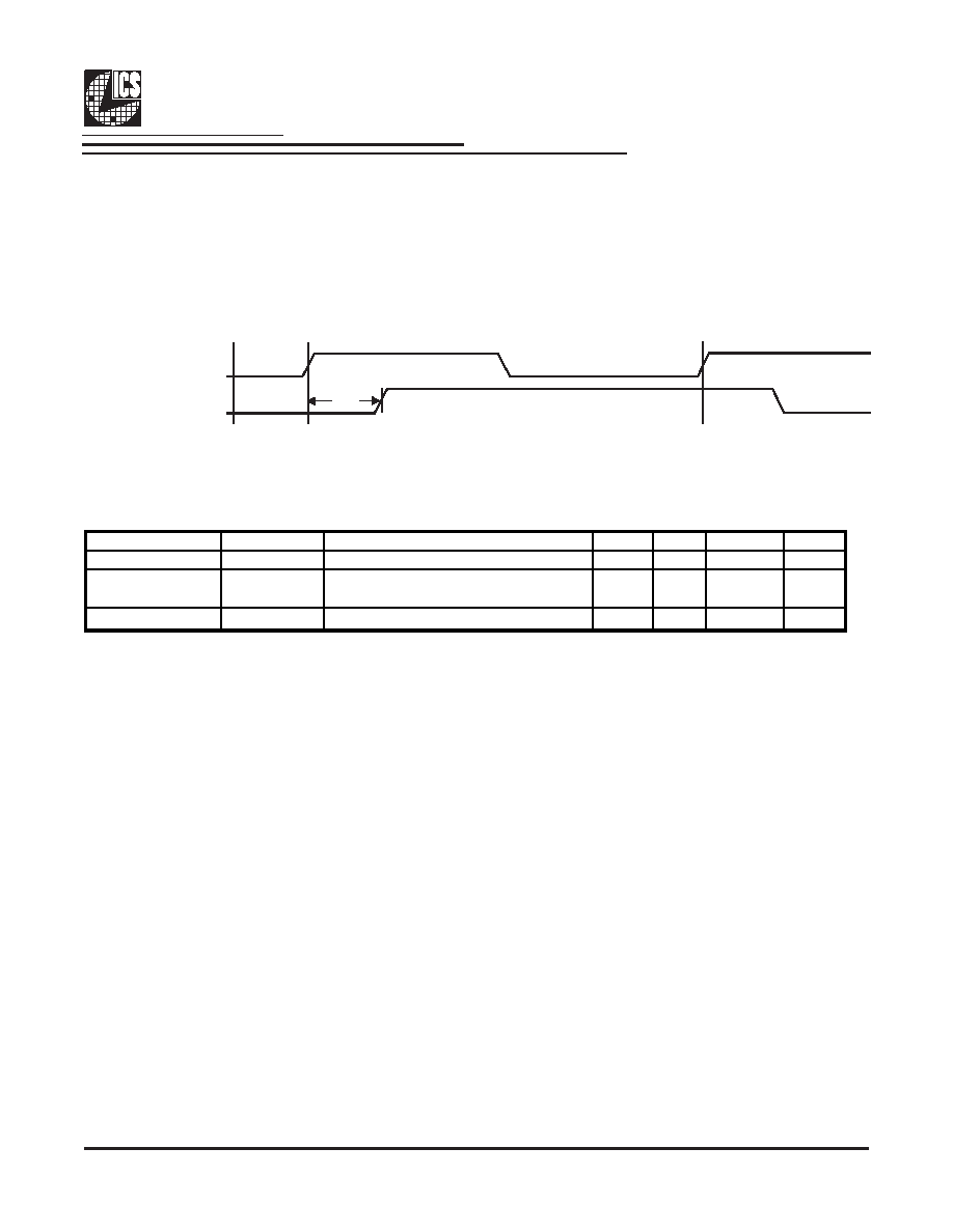
All 3V66 clocks are to be in pphase with each other. In the case where 3V66_1 is configured as 48MHz VCH clock, there is no
defined phase relationship between 3V66_1/VCH and other 3V66 clocks. The PCI group should lag 3V66 by the standard
skew described below as Tpci.
Un-Buffered Mode 3V66 & PCI Phase Relationship
3V66
PCICLK_F and PCICLK
Tpci
Group Skews at Common Transition Edges
GROUP
SYMBOL
CONDITIONS
MIN
TYP
MAX
UNITS
3V66
3V66 (5:0) pin to pin skew
0
250
ps
PCI
PCI_F (2:0) and
PCI (6:0) pin to pin skew
0
500
ps
3V66 to PCI
S3V66-PCI
3V66 (5:0) leads 33MHz PCI
1.5
3.5
ns
1Guaranteed by design, not 100% tested in production.
发布紧急采购,3分钟左右您将得到回复。
相关PDF资料
ICS950908BFLF
IC TIMING CTRL HUB P4 56-SSOP
ICS951402AGLF
IC TIMING CTRL HUB P4 48-TSSOP
ICS95V847AGIT
IC CLOCK DRIVER 2.5V 24-TSSOP
ICS95V850AGT
IC CLK DVR PLL 1:10 48TSSOP
ICS95V857ALT
IC CLK DVR PLL 1:10 40TVSOP
ICS95V857CKLF8
IC CLK DVR PLL 1:10 40VFQFN
ICS97U870AKT
IC CLK DVR PLL 1:10 40VFQFN
ICS97ULP877AHT
IC CLOCK DRIVER 1.8V LP 52-BGA
相关代理商/技术参数
ICS950218AFLF
功能描述:IC TIMING CTRL HUB P4 48-SSOP RoHS:是 类别:集成电路 (IC) >> 时钟/计时 - 专用 系列:TCH™ 标准包装:28 系列:- 类型:时钟/频率发生器 PLL:是 主要目的:Intel CPU 服务器 输入:时钟 输出:LVCMOS 电路数:1 比率 - 输入:输出:3:22 差分 - 输入:输出:无/是 频率 - 最大:400MHz 电源电压:3.135 V ~ 3.465 V 工作温度:0°C ~ 85°C 安装类型:表面贴装 封装/外壳:64-TFSOP (0.240",6.10mm 宽) 供应商设备封装:64-TSSOP 包装:管件
ICS950218AFLFT
功能描述:IC TIMING CTRL HUB P4 48-SSOP RoHS:是 类别:集成电路 (IC) >> 时钟/计时 - 专用 系列:TCH™ 标准包装:28 系列:- 类型:时钟/频率发生器 PLL:是 主要目的:Intel CPU 服务器 输入:时钟 输出:LVCMOS 电路数:1 比率 - 输入:输出:3:22 差分 - 输入:输出:无/是 频率 - 最大:400MHz 电源电压:3.135 V ~ 3.465 V 工作温度:0°C ~ 85°C 安装类型:表面贴装 封装/外壳:64-TFSOP (0.240",6.10mm 宽) 供应商设备封装:64-TSSOP 包装:管件
ICS950218AFT
功能描述:IC TIMING CTRL HUB P4 48-SSOP RoHS:否 类别:集成电路 (IC) >> 时钟/计时 - 专用 系列:TCH™ 标准包装:1,500 系列:- 类型:时钟缓冲器/驱动器 PLL:是 主要目的:- 输入:- 输出:- 电路数:- 比率 - 输入:输出:- 差分 - 输入:输出:- 频率 - 最大:- 电源电压:3.3V 工作温度:0°C ~ 70°C 安装类型:表面贴装 封装/外壳:28-SSOP(0.209",5.30mm 宽) 供应商设备封装:28-SSOP 包装:带卷 (TR) 其它名称:93786AFT
ICS950218YFLF-T
制造商:ICS 制造商全称:ICS 功能描述:Programmable Timing Control Hub TM for P4 TM
ICS950220
制造商:ICS 制造商全称:ICS 功能描述:Programmable Timing Control Hub⑩ for P4⑩
ICS950220AFLF
功能描述:IC TIMING CTRL HUB P4 48-SSOP RoHS:是 类别:集成电路 (IC) >> 时钟/计时 - 专用 系列:TCH™ 标准包装:28 系列:- 类型:时钟/频率发生器 PLL:是 主要目的:Intel CPU 服务器 输入:时钟 输出:LVCMOS 电路数:1 比率 - 输入:输出:3:22 差分 - 输入:输出:无/是 频率 - 最大:400MHz 电源电压:3.135 V ~ 3.465 V 工作温度:0°C ~ 85°C 安装类型:表面贴装 封装/外壳:64-TFSOP (0.240",6.10mm 宽) 供应商设备封装:64-TSSOP 包装:管件
ICS950220AFLFT
功能描述:IC TIMING CTRL HUB P4 48-SSOP RoHS:是 类别:集成电路 (IC) >> 时钟/计时 - 专用 系列:TCH™ 标准包装:28 系列:- 类型:时钟/频率发生器 PLL:是 主要目的:Intel CPU 服务器 输入:时钟 输出:LVCMOS 电路数:1 比率 - 输入:输出:3:22 差分 - 输入:输出:无/是 频率 - 最大:400MHz 电源电压:3.135 V ~ 3.465 V 工作温度:0°C ~ 85°C 安装类型:表面贴装 封装/外壳:64-TFSOP (0.240",6.10mm 宽) 供应商设备封装:64-TSSOP 包装:管件
ICS950220YFLFT
制造商:ICS 制造商全称:ICS 功能描述:Programmable Timing Control Hub⑩ for P4⑩